SPI Bus and the ST7789 Display
Slides: here
Theory
The Serial Peripheral Interface (SPI)
Serial Peripheral Interface (SPI) is a synchronous, full-duplex serial communication bus that is widely adopted in embedded systems for connecting processors to peripheral devices including displays, ADCs, DACs, flash memories, sensors and more. SPI is designed for short distance communication and supports clock frequencies ranging from few MHz for sensors to 50-100+ MHz for high performance devices such as SPI flash memories.
SPI Signals
On an SPI bus, one device acts as the master initiating all the communication by generating the clock signal and selecting the target device. The remaining devices act as slaves and respond only when selected.
A typical master is a microcontroller, microprocessor or a System-on-Chip (SoC) while common slave devices include sensors, analog-to-digital converters (ADCs), digital-to-analog converters (DACs), displays and flash memories.
A standard SPI bus uses four signals:
Signal |
Direction |
Description |
|---|---|---|
SCLK |
Master -> Slave |
Serial clock generated by the master |
MOSI |
Master -> Slave |
Master Out Slave In. Data sent from the master to the slave |
MISO |
Slave -> Master |
Master In Slave Out. Data sent from the slave to the master |
CS/SS |
Master -> Slave |
Chip Select (active low) |
Note
Modern documentation increasingly uses the terms controller and peripheral (or host and device) instead of master and slave. However, the traditional terminology and signal names (MOSI, MISO, SS) are still widely encountered in datasheets and technical literature.
Multiple devices may share SCLK, MOSI, and MISO, each with its own CS# line:
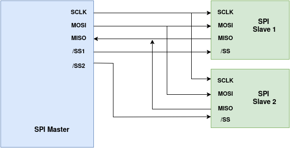
Figure 21 Typical SPI signals: Master and two slave devices
The Serial Clock (SCLK)
The Serial Clock (SCLK) signal is generated by the master device. As a result, slave devices do not need their own clock source and they will use the clock generated by the master device.
SPI doesn’t have a standardized clock rate but typically operates in the MHz range. The purpose of the clock is to indicate to the receiver when data should be sampled. Each clock cycle corresponds to one bit of data being transferred.
Depending on the SPI configuration:
The clock can remain idle low or idle high.
Data can be sampled on either the rising edge or the falling edge of the clock signal.
Clock Polarity
Clock polarity (CPOL) defines the idle state of the SCLK line, that is the level when the clock is idle (when the bus is not transferring data).
CPOL=0, SCLK idles LOW. The first clock transition after CS asserts is therefore a rising edge.
CPOL=1, SCLK idles HIGH. The first clock transition after CS asserts is therefore a falling edge.
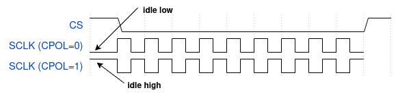
Figure 22 SPI Clock Polarity (CPOL)
Clock Phase
Clock Phase (CPHA) determines which edge of the clock signal is used to read (sample) or write (shift) the data.
CPHA=0, data is sampled on the leading (first) edge of each clock pulse and shifted out on the trailing edge.
CPHA=1, data is shifted out on the leading edge and sampled on the trailing (second) edge.
CPOL and CPHA combine into four modes:
CPOL |
CPHA |
Mode |
Behaviour |
|---|---|---|---|
0 |
0 |
Mode 0 |
SCLK idles low, shifted on falling edge, sampled on rising edge. Default in Linux |
0 |
1 |
Mode 1 |
SCLK idles low, shifted on rising edge, sampled on falling edge. |
1 |
0 |
Mode 2 |
SCLK idles high, shifted on rising edge, sampled on falling edge. |
1 |
1 |
Mode 3 |
SCLK idles high, shifted on falling edge, sampled on rising edge. |
SPI Transaction
A typical SPI one byte transmission starts with master asserting CS# low to select the slave device. Once CS# is asserted, the master starts generating SCLK clock signal. Data is driven by the master on the MOSI line, transmitted MSB first: bit 7 (most significant) is placed on the MOSI line first and bit 0 (least significant) is placed last. Once all the 8 bits have been clocked out, the master stops the clock and drives the CS# high signalling the end of transmission.

Figure 23 SPI single byte transmission (Mode 0, MSB first)
Overview
The ST7789VW (Sitronix) is a single-chip TFT-LCD controller with on-chip frame memory. Key characteristics, see datahseet:
Maximum resolution: 240 (H) × 320 (V) RGB pixels
On-chip frame buffer: 240 × 320 × 18 bits
Pixel formats: 12 bpp (RGB444), 16 bpp (RGB565), 18 bpp (RGB666)
4-wire SPI interface (SCL, SDA, CS, DCX) — no MISO needed for display use
Operating supply: 3.3 V
The 240×240 module physically crops the 240×320 controller to 240 rows
ST7789 Interface Pins (SPI 4-Line Mode)
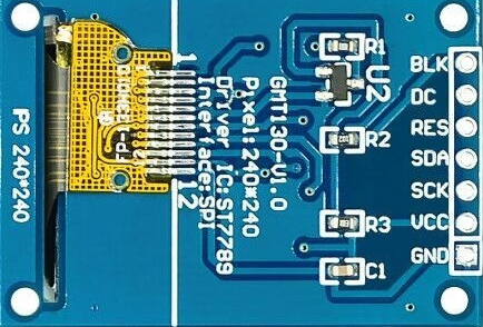
Figure 24 ST7789V TFT display, 240 x 240
Pin Name |
Direction |
Description |
|---|---|---|
GND |
Power |
Ground reference. |
VCC |
Power |
Connect to 3.3 V only. |
SCL (SCK) |
Input |
Serial clock. Maximum write frequency 62.5 MHz |
SDA (MOSI) |
Input |
Serial data in. Clocked on rising edge of SCL (SPI Mode 0). |
RES |
Input |
Hardware reset, active-low. |
DC |
Input |
Data / Command select. LOW = command HIGH = data |
BLK |
Input |
Backlight enable. Connect to 3.3 V for always-on backlight. |
CS |
Input |
Chip select, active-low. Tied to GND on the module (always selected). |
4-Line SPI Protocol: Command vs. Data
The defining feature of the 4-line SPI protocol is the DCX signal, which tells the controller whether each incoming byte is a command opcode or a data parameter / pixel byte:

Figure 25 DCX set LOW for commmand, HIGH for parameters/data
The diagram above shows a complete CASET (Column Address Set) transaction
on the SPI bus. CASET is command 0x2A and must be sent before every
RAMWR pixel write to define the horizontal drawing window.
The transaction consists of five bytes sent in a single CS assertion:
CSX is pulled low for the entire transaction and released only after the last parameter byte.
DCX is held low during the first byte only, telling the ST7789V that
0x2Ais a command. It then goes high and stays high for the four parameter bytes that follow.SDA carries the five bytes in sequence, MSB first:
Byte
Value
Meaning
Command
0x2A
CASET, column address set
SC high
0x00
Start column high byte
SC low
0x00
Start column low byte
EC high
0x00
End column high byte
EC low
0xEF
End column low byte (239)
After this transaction the ST7789V drawing window spans all 240 columns
from the left edge (column 0) to the right edge (column 239). A
subsequent RASET (0x2B) sets the row range and RAMWR
(0x2C) begins the pixel data stream into the defined window.
ST7789 GRAM and Address Window
The ST7789V has internal Display Data RAM (GRAM) organised as a 240x240 grid of pixels (240 rows by 240 columns).
Before writing any pixel data the ST7789V must know exactly which region of GRAM to fill. This is done by sending three commands in sequence:
CASET (0x2A) defines the horizontal boundaries of the write window by specifying a pair of column addresses: SC (Start Column) sets the left edge and EC (End Column) sets the right edge. Any column address outside the (SC, EC) pair is not written.
RASET (0x2B) defines the vertical boundaries by specifying a pair of row addresses: SR (Start Row) sets the top edge and ER (End Row) sets the bottom edge. Any row address outside the (SR, ER) pair is not written.
Together (SC, EC) and (SR, ER) define a rectangular write window inside GRAM. Once both commands have been sent, RAMWR (0x2C) opens the pixel data stream. The controller writes incoming pixels into the window starting at (SC, SR), the top-left corner and auto-increments the write pointer left to right across each row, then moves to the next row down, until the bottom-right corner (EC, ER) is reached.
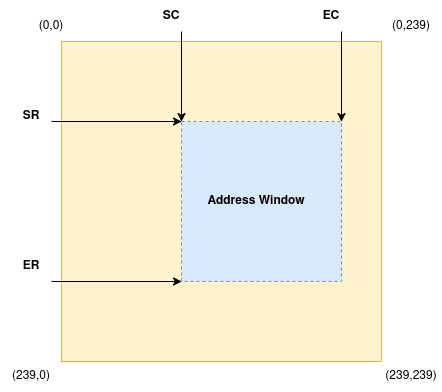
Figure 26 ST7789V - 240 x 240 GRAM address window
ST7789 Initialization Sequence
After hardware reset the controller is in sleep mode. The essential bring-up sequence is:
st7789_hw_reset(priv);
st7789_init_display(priv)
Where we need to reset the chip by drive RESX LOW > 15 ms, then HIGH; wait > 120 ms.
static void st7789_hw_reset(struct st7789_priv *priv)
{
    gpiod_set_value(priv->reset, 1);   /* assert RESX LOW (active-low) */
    msleep(20);                         /* hold > 15 ms */
    gpiod_set_value(priv->reset, 0);   /* deassert RESX HIGH */
    msleep(150);                        /* wait> 120 ms before cmds */
}
And them perform minimal initializaton sequence as below:
static int st7789_init_display(struct st7789_priv *priv)
{

  st7789_write_cmd(priv, ST7789_SLPOUT);    /* exit sleep; wait 500ms */
  msleep(500);
  st7789_write_cmd(priv, ST7789_COLMOD);    /* pixel format           */
  st7789_write_data_byte(priv, 0x55);       /* 0x55 = RGB565          */
  st7789_write_cmd(priv, ST7789_MADCTL);    /* memory access control  */
  st7789_write_data_byte(priv, 0x00);       /* normal orientation     */
  st7789_write_cmd(priv, ST7789_INVON);     /* inversion on           */
  st7789_write_cmd(priv, ST7789_NORON);     /* normal display mode    */
  st7789_write_cmd(priv, ST7789_DISPON);    /* display on; wait 100ms */
  msleep(100);
  return 0;
}
Essential ST7789 Commands
Mnemonic |
Opcode |
Params |
Description |
|---|---|---|---|
SWRESET |
0x01 |
0 |
Software reset. Wait > 150 ms after issuing. |
SLPOUT |
0x11 |
0 |
Exit sleep mode. Wait > 500 ms after issuing. |
INVOFF |
0x20 |
0 |
Display inversion off. |
INVON |
0x21 |
0 |
Display inversion on (required on most ST7789 modules). |
DISPOFF |
0x28 |
0 |
Display off. Output blanked, GRAM retained. |
DISPON |
0x29 |
0 |
Display on. Wait > 100 ms after issuing. |
CASET |
0x2A |
4 |
Column address set: SC_H, SC_L, EC_H, EC_L (big-endian pairs defining the column window). |
RASET |
0x2B |
4 |
Row address set: SR_H, SR_L, ER_H, ER_L (big-endian pairs defining the row window). |
RAMWR |
0x2C |
N |
Memory write. All subsequent bytes are pixel data filling the window defined by CASET and RASET. |
MADCTL |
0x36 |
1 |
Memory access control: rotation, mirror, RGB/BGR order. Controls physical (0,0) origin. |
COLMOD |
0x3A |
1 |
Pixel format. 0x55 = RGB565 (16 bpp), 0x66 = RGB666 (18 bpp). |
PORCTRL |
0xB2 |
5 |
Porch control (front/back porch timing). |
GCTRL |
0xB7 |
1 |
Gate control (VGH/VGL switching speed). |
VCOMS |
0xBB |
1 |
VCOM voltage setting. |
PWCTRL1 |
0xD0 |
2 |
Power control 1 (AVDD, AVCL, VDS). |
PVGAMCTRL |
0xE0 |
14 |
Positive voltage gamma control curve. |
NVGAMCTRL |
0xE1 |
14 |
Negative voltage gamma control curve. |
Complete initialization function:
static int st7789_init_display(struct st7789_priv *priv)
{
        static const u8 porctrl[]   = { 0x05, 0x05, 0x00, 0x33, 0x33 };
        static const u8 vdvvrhen[]  = { 0x01, 0xFF };
        static const u8 pwctrl1[]   = { 0xA4, 0xA1 };
        static const u8 pvgamctrl[] = { 0xD0, 0x05, 0x0A, 0x09, 0x08, 0x05, 0x2E,
                                        0x44, 0x45, 0x0F, 0x17, 0x16, 0x2B, 0x33 };
        static const u8 nvgamctrl[] = { 0xD0, 0x05, 0x0A, 0x09, 0x08, 0x05, 0x2E,
                                        0x43, 0x45, 0x0F, 0x16, 0x16, 0x2B, 0x33 };
        int ret;

        ret = st7789_write_cmd(priv, ST7789_SLPOUT);
        if (ret) return ret;
        msleep(600);

        ret = st7789_write_cmd(priv, ST7789_COLMOD);
        if (ret) return ret;
        ret = st7789_write_data_byte(priv, ST7789_COLMOD_RGB565);
        if (ret) return ret;

        ret = st7789_write_cmd(priv, ST7789_PORCTRL);
        if (ret) return ret;
        ret = st7789_write_data(priv, porctrl, sizeof(porctrl));
        if (ret) return ret;

        ret = st7789_write_cmd(priv, ST7789_GCTRL);
        if (ret) return ret;
        ret = st7789_write_data_byte(priv, 0x75);
        if (ret) return ret;

        ret = st7789_write_cmd(priv, ST7789_VDVVRHEN);
        if (ret) return ret;
        ret = st7789_write_data(priv, vdvvrhen, sizeof(vdvvrhen));
        if (ret) return ret;

        ret = st7789_write_cmd(priv, ST7789_VRHS);
        if (ret) return ret;
        ret = st7789_write_data_byte(priv, 0x13);
        if (ret) return ret;

        ret = st7789_write_cmd(priv, ST7789_VDVS);
        if (ret) return ret;
        ret = st7789_write_data_byte(priv, 0x20);
        if (ret) return ret;

        ret = st7789_write_cmd(priv, ST7789_VCOMS);
        if (ret) return ret;
        ret = st7789_write_data_byte(priv, 0x22);
        if (ret) return ret;

        ret = st7789_write_cmd(priv, ST7789_VCMOFSET);
        if (ret) return ret;
        ret = st7789_write_data_byte(priv, 0x20);
        if (ret) return ret;

        ret = st7789_write_cmd(priv, ST7789_PWCTRL1);
        if (ret) return ret;
        ret = st7789_write_data(priv, pwctrl1, sizeof(pwctrl1));
        if (ret) return ret;

        ret = st7789_write_cmd(priv, ST7789_DISPON);
        if (ret) return ret;
        msleep(150);

        ret = st7789_write_cmd(priv, ST7789_INVON);
        if (ret) return ret;

        ret = st7789_write_cmd(priv, ST7789_MADCTL);
        if (ret) return ret;
        ret = st7789_write_data_byte(priv, ST7789_MADCTL_NORMAL);
        if (ret) return ret;

        ret = st7789_write_cmd(priv, ST7789_PVGAMCTRL);
        if (ret) return ret;
        ret = st7789_write_data(priv, pvgamctrl, sizeof(pvgamctrl));
        if (ret) return ret;

        ret = st7789_write_cmd(priv, ST7789_NVGAMCTRL);
        if (ret) return ret;
        ret = st7789_write_data(priv, nvgamctrl, sizeof(nvgamctrl));
        if (ret) return ret;

        return 0;
}
RGB565 Pixel Format
RGB565 Bit Layout
RGB565 encodes one pixel into 16 bits spread across two bytes. The
high byte (sent first over SPI) carries the 5 red bits in its upper
half and the top 3 bits of green in its lower half. The low byte
(sent second) carries the remaining 3 bits of green followed by the 5
blue bits. Green gets 6 bits instead of 5 because the human eye is most
sensitive to green and the extra bit doubles its resolution. The full
16-bit value is assembled as pixel = (R << 11) | (G << 5) | B,
giving 32 levels of red, 64 levels of green, and 32 levels of blue —
65,536 colours in total.

Figure 27 RGB565 format - encodes (R, G, B) values into 2 bytes
Common color constants:
Color |
RGB565 value |
Components (R, G, B) |
|---|---|---|
Red |
|
R=31 (max), G=0, B=0 |
Green |
|
R=0, G=63 (max), B=0 |
Blue |
|
R=0, G=0, B=31 (max) |
White |
|
R=31 (max), G=63 (max), B=31 (max) |
Black |
|
R=0, G=0, B=0 |
Yellow |
|
R=31 (max), G=63 (max), B=0 |
Cyan |
|
R=0, G=63 (max), B=31(max) |
Magenta |
|
R=31 (max), G=0, B=31(max) |
ST7789 Driver Functions Reference
This section provides complete, copy-pasteable implementations of every function students must implement. Use these as a reference, read and understand each function before implementing it yourself in the skeleton.
Low-level SPI Primitives
The two fundamental building blocks are st7789_write_cmd() and
st7789_write_data(). Every higher-level function calls one or both of these.
The DCX (D/C) GPIO determines whether the byte being clocked is a command opcode or a data byte.
Writing command 0x2C (RAMWR):
  Step 1: gpiod_set_value(dc, 0)  -> DCX = LOW  = command
  Step 2: spi_write(spi, &0x2C, 1)

Writing 2 data bytes {0xF8, 0x00} (one red pixel):
  Step 1: gpiod_set_value(dc, 1)     -> DCX = HIGH = data
  Step 2: spi_write(spi, buf, 2)
/* Set DCX LOW then clock the command opcode. */
static int st7789_write_cmd(struct st7789_priv *priv, u8 cmd)
{
    gpiod_set_value(priv->dc, 0);
    return spi_write(priv->spi, &cmd, 1);
}

/* Set DCX HIGH then clock len data bytes. */
static int st7789_write_data(struct st7789_priv *priv,
                             const u8 *buf, size_t len)
{
    gpiod_set_value(priv->dc, 1);
    return spi_write(priv->spi, buf, len);
}

/* Convenience wrapper: send a single data byte. */
static inline int st7789_write_data_byte(struct st7789_priv *priv, u8 byte)
{
    return st7789_write_data(priv, &byte, 1);
}
Hardware Reset
The reset line is declared GPIO_ACTIVE_LOW in the device tree and obtained
with GPIOD_OUT_HIGH (i.e., deasserted on boot). To assert reset we write
logical 1 (the gpiod layer inverts to physical LOW):
static void st7789_hw_reset(struct st7789_priv *priv)
{
    gpiod_set_value(priv->reset, 1);   /* assert RESX LOW (active-low) */
    msleep(20);                         /* hold > 15 ms                */
    gpiod_set_value(priv->reset, 0);   /* deassert RESX HIGH           */
    msleep(150);                        /* wait > 120 ms before cmds   */
}
Address Window: st7789_set_addr_win
The address window defines the rectangular region of GRAM that subsequent RAMWR pixel data will fill. CASET sets the column (X) range; RASET sets the row (Y) range. Each takes four bytes encoding two big-endian 16-bit values:
CASET parameter encoding for x0=0, x1=239:

Byte 0: x0 >> 8  = 0x00    ->start column (big-endian)
Byte 1: x0 & 0xFF= 0x00
Byte 2: x1 >> 8  = 0x00    -> end column (big-endian)
Byte 3: x1 & 0xFF= 0xEF       (239 = 0x00EF)

RASET parameter encoding for y0=10, y1=49 (a 40-row band):

Byte 0: 0x00   -> start row = 10 = 0x000A
Byte 1: 0x0A
Byte 2: 0x00   -> end row   = 49 = 0x0031
Byte 3: 0x31

After CASET + RASET, send RAMWR to open the pixel data stream.
Pixel data then fills the window left-to-right, top-to-bottom.
static int st7789_set_addr_win(struct st7789_priv *priv,
                               u16 x0, u16 y0, u16 x1, u16 y1)
{
    u8 col[4] = { x0 >> 8, x0 & 0xff, x1 >> 8, x1 & 0xff };
    u8 row[4] = { y0 >> 8, y0 & 0xff, y1 >> 8, y1 & 0xff };
    int ret;

    ret = st7789_write_cmd(priv, ST7789_CASET);
    if (ret) return ret;
    ret = st7789_write_data(priv, col, 4);
    if (ret) return ret;

    ret = st7789_write_cmd(priv, ST7789_RASET);
    if (ret) return ret;
    ret = st7789_write_data(priv, row, 4);
    if (ret) return ret;

    return st7789_write_cmd(priv, ST7789_RAMWR);
}
Full-screen Fill: st7789_fill
st7789_fill() paints the entire panel with a single color. The naive approach
of calling st7789_draw_pixel() 240 x 240 = 57600 times would issue 172,800 SPI
transactions (3 per pixel: CASET + RASET + RAMWR). Instead, we:
Set one full-panel address window (3 SPI transactions total).
Allocate one scanline buffer (
width * 2bytes) and fill it with the repeated color.Send that buffer once per row (240 SPI transactions of 480 bytes each).
static int st7789_fill(struct st7789_priv *priv, u16 color)
{
    u8 color_hi = color >> 8;
    u8 color_lo = color & 0xff;
    u8 *line;
    int ret = 0, x, y;

    ret = st7789_set_addr_win(priv, 0, 0, priv->width - 1, priv->height - 1);
    if (ret) return ret;

    line = kmalloc(priv->width * 2, GFP_KERNEL);
    if (!line) return -ENOMEM;

    /* Build one scanline of the repeated color in big-endian */
    for (x = 0; x < priv->width; x++) {
        line[x * 2]     = color_hi;
        line[x * 2 + 1] = color_lo;
    }

    /* Send the scanline once per row */
    for (y = 0; y < priv->height; y++) {
        ret = st7789_write_data(priv, line, priv->width * 2);
        if (ret) break;
    }

    kfree(line);
    return ret;
}
Single Pixel: st7789_draw_pixel
A pixel is a 1×1 address window. Set CASET(x,x) RASET(y,y) then send the two-byte RGB565 value. Note: the ST7789 expects big-endian — high byte first.
For pixel color 0x07FF (cyan):
  Byte sent 1st: 0x07   (bits 15:8 of 0x07FF)
  Byte sent 2nd: 0xFF   (bits  7:0 of 0x07FF)
static int st7789_draw_pixel(struct st7789_priv *priv,
                             u16 x, u16 y, u16 color)
{
    u8 pixel[2] = { color >> 8, color & 0xff };
    int ret;

    if (x >= priv->width || y >= priv->height) return 0;

    ret = st7789_set_addr_win(priv, x, y, x, y);
    if (ret) return ret;
    return st7789_write_data(priv, pixel, 2);
}
Filled Rectangle: st7789_fill_rect
st7789_fill_rect() is a generalisation of st7789_fill(): the address window
is an arbitrary sub-rectangle instead of the full screen. Coordinate clamping
ensures callers do not need to range-check their arguments:
static int st7789_fill_rect(struct st7789_priv *priv,
                            u16 x, u16 y, u16 w, u16 h, u16 color)
{
    u8 color_hi = color >> 8;
    u8 color_lo = color & 0xff;
    u8 *line;
    int ret = 0;
    u16 i, row;

    /* Clamp to panel boundaries */
    if (x >= priv->width || y >= priv->height) return 0;
    if (x + w > priv->width)  w = priv->width  - x;
    if (y + h > priv->height) h = priv->height - y;

    ret = st7789_set_addr_win(priv, x, y, x + w - 1, y + h - 1);
    if (ret) return ret;

    line = kmalloc(w * 2, GFP_KERNEL);
    if (!line) return -ENOMEM;

    for (i = 0; i < w; i++) {
        line[i * 2]     = color_hi;
        line[i * 2 + 1] = color_lo;
    }
    for (row = 0; row < h; row++) {
        ret = st7789_write_data(priv, line, w * 2);
        if (ret) break;
    }

    kfree(line);
    return ret;
}
Physical Wiring
Connect the ST7789 display module (7-pin breakout) to the EXT2 header (J601) as shown below. Use jumper wires and a bread board for a first setup then use the LKSS daughter board.
Display Module Pin |
EXT2 (J601) Pin |
SoC Pad |
Notes |
|---|---|---|---|
VCC |
Pin 1 (3.3 V) |
Never connect to 5 V. |
|
GND |
Pin 39 (GND) |
Ground |
|
BLK (backlight) |
Pin 1 (3.3 V) |
Tie high for always-on backlight. |
|
SCL (clock) |
Pin 40 |
GPIO_IO21 |
LPSPI4_SCK; driven by GPIO2_IO21 |
SDA (MOSI) |
Pin 38 |
GPIO_IO20 |
LPSPI4_SOUT; driven by GPIO2_IO20 |
RES (reset) |
Pin 37 |
GPIO_IO19 |
Active-low; driven by GPIO2_IO19 |
DC (data/cmd) |
Pin 33 |
GPIO_IO13 |
Active-high = data; driven by GPIO2_IO13 |
CS |
GND (module internal) |
Module CS is soldered to GND on the PCB. |
Warning
Double-check VCC before powering on. Applying 5 V to the ST7789 module will permanently damage the display controller.
Device Tree
Two device tree nodes are required:
An
&lpspi4bus node activating the LPSPI4 controller.An
st7789child node describing the display as an SPI device.
Add the following fragment to
repos/lkss-linux/arch/arm64/boot/dts/freescale/imx93-11x11-frdm.dts:
&lpspi4 {
    #address-cells = <1>;
    #size-cells    = <0>;
    status         = "okay";

    pinctrl-0    = <&pinctrl_lpspi4_st7789>;
    pinctrl-names = "default";

    lkss_st7789: st7789@0 {
        compatible        = "lkss,st7789";
        reg               = <0>;            /* chip-select index 0   */
        spi-max-frequency = <62500000>;

        /* D/C:   GPIO2_IO13 (J601 pin 22), active-high = data */
        dc-gpios    = <&gpio2 13 GPIO_ACTIVE_HIGH>;

        /* Reset: GPIO2_IO19 (J601 pin 15), active-low */
        reset-gpios = <&gpio2 19 GPIO_ACTIVE_LOW>;
    };
};

&iomuxc {
    pinctrl_lpspi4_st7789: lpspi4-st7789grp {
        fsl,pins = <
            MX93_PAD_GPIO_IO21__LPSPI4_SCK   0x31e   /* J601 pin 16, SCK  */
            MX93_PAD_GPIO_IO20__LPSPI4_SOUT  0x31e   /* MOSI              */
            MX93_PAD_GPIO_IO13__GPIO2_IO13   0x31e   /* J601 pin 22, D/C  */
            MX93_PAD_GPIO_IO19__GPIO2_IO19   0x31e   /* J601 pin 15, RST  */
        >;
    };
};
Lab Exercises
Note
The lab source code lives in the Linux kernel tree under
repos/lkss-linux/drivers/lkss/lab3/.
Before each test cycle the workflow is:
Edit/write your driver in
repos/lkss-linux/drivers/lkss/lab3/Select config option to build your code as a module
M$ ./scripts/lkss.py menuconfigCompile the module and copy them to rootfs
$ ./scripts/lkss.py compile --install-modulesIn a separate terminal open the serial console
$ minicom -D /dev/ttyACM0Boot the board
$ ./scripts/lkss.py bootLoad the module and observe
$ modprobe your_module.koUnload the module (if requested)
$ rmmod your_module.ko
1. Wire the Hardware
Connect the ST7789 display module to the i.MX93 FRDM board.
Note
If you are using the LKSS daugther board, insert the ST7789 display into the corresponding location indicated by the J4 pin header and then go to next exercise.
Using the wiring table in Physical Wiring, connect the 7-pin display module to the EXT2 header (J601) using short jumper wires.
Double-check VCC goes to 3.3 V only. Connect BLK to 3.3 V for always-on backlight.
The display should power on (backlight on) as soon as 3.3 V is applied, but will show nothing until the driver initializes it.
Warning
Never apply 5 V to VCC or any signal pin. Doing so will permanently destroy the display controller.
2. Add the Device Tree Node
Open the i.MX93 FRDM dts file:
repos/lkss-linux/arch/arm64/boot/dts/freescale/imx93-11x11-frdm.dtsAdd the
&lpspi4and&iomuxcpinctrl_lpspi4_st7789nodes from Device Tree.Recompile and boot:
$ ./scripts/lkss.py compile
$ ./scripts/lkss.py boot
On the board, verify the SPI device appeared:
ls /sys/bus/spi/devices/
You should see an entry like
spi0.0. The bus number is assigned by the kernel in probe order, not by the LPSPI controller number.Inspect the compatible string at runtime:
cat /sys/bus/spi/devices/spi0.0/of_node/compatible
# Expected: lkss,st7789
3. Build and Load the driver skeleton
Compile and load the st7789.c skeleton driver. Check that st7789.c probe() function is called.
Enable the driver:
./scripts/lkss.py menuconfig
# select M to compile the st7789.c driver as a module
# Device Drivers -> Linux Kernel Summer School Drivers -> LKSS Lab 3 drivers -> ST7789 SPI display
Build and install st7789.c driver:
./scripts/lkss.py compile --install-modules
Load the driver:
modprobe st7789.ko
dmesg | grep -i st7789
The skeleton has empty stubs for all functions (exercises 4–9). After loading you should see:
[  118.615213] st7789 spi0.0: ST7789 probe: speed=62500000 Hz
[  118.625000] st7789 spi0.0: ST7789 ready
The display stays dark until exercises 4–6 are implemented. If an error appears instead, check your DT node and GPIO wiring.
4. Low-level SPI Primitives
Reference: Low-level SPI Primitives.
Open st7789.c and find TODO 4.1, TODO 4.2, and TODO 4.3.
Copy the three functions from the theory section:
TODO 4.1 –
st7789_write_cmd(): set DCX LOW then callspi_write().TODO 4.2 –
st7789_write_data(): set DCX HIGH then callspi_write().TODO 4.3 –
st7789_write_data_byte(): callwrite_data()with&byte, 1.
After implementing, make sure you understand:
Why DCX must be driven before
spi_write().Why
st7789_write_data_byte()is a convenience wrapper and not a separate SPI transaction.What happens if you swap the DCX logic (LOW for data, HIGH for command)?
Question: What is the minimum number of SPI transactions needed to send one ST7789 command with 4 data bytes? (Answer: 2 — one for the command byte with DCX=LOW, one for all 4 data bytes with DCX=HIGH.)
5. Hardware Reset
Reference: Hardware Reset.
Open st7789.c and find TODO 5. Copy st7789_hw_reset() from the
theory section and answer:
Why does writing logical
1topriv->resetdrive the physical pin LOW? (Hint:reset-gpiosin the DT usesGPIO_ACTIVE_LOW.)What would happen if you forgot the 150 ms sleep after deasserting reset?
The probe function calls
st7789_hw_reset(priv)beforest7789_init_display(). Why must reset happen first?
6. Initialization Sequence
Reference: Look at ST7789 initialization sequence in order to do perform minimal display init.
Open st7789.c and find TODO 6. Copy the minimal st7789_init_display
initialization sequence from the theory section. The sequence should be enough
for simple primitives.
When switching to more complex scence please use the complete initialization sequence. It configures PORCTRL, GCTRL, VCOMS, VDVVRHEN, VRHS, VDVS, VCMOFSET, PWCTRL1, PVGAMCTRL, and NVGAMCTRL for correct colour and contrast.
Test: After implementing exercises 4–6, rebuild and reload the module.
The display should wake up. The color cycle (exercise 7) will confirm
red, green, and blue once fill() is implemented.
7. Address Window and Fill
Reference: Address Window and Full-screen Fill.
Open st7789.c and find TODO 7.1 and TODO 7.2. Copy the two
functions from the theory section:
TODO 7.1 –
st7789_set_addr_win(): send CASET + RASET + RAMWR with 4-byte big-endian coordinates.TODO 7.2 –
st7789_fill(): set the full-panel address window, allocate one scanline buffer, fill it with the repeated color, and send it once per row.
After implementing, answer:
Why are the column/row coordinates encoded as 4-byte big-endian pairs even though the CPU is little-endian?
st7789_fill()allocates one scanline buffer and sends itheighttimes rather than allocating the full pixel buffer. What is the memory saving for a 240×240 display? (Answer: 240×480 B vs. 480 B.)After
st7789_set_addr_win()there is no CS# de-assert between CASET, RASET, and RAMWR, why not?
Test: After exercises 4–7 are done, st7789_demo() shows a solid red
screen, then green, then blue.
8. Filled Rectangle
Reference: Filled Rectangle.
Open st7789.c and find TODO 8. Copy st7789_fill_rect() from the
theory section and explain:
Why is the clamping check
if (x + w > priv->width) w = priv->width - xnecessary? What would happen without it?How does
fill_rect(x, y, 240, 4, color)differ fromfill(color)in terms of the CASET/RASET parameters sent to the display?Trace the CASET/RASET values for the top border call in
st7789_demo():fill_rect(0, 0, 240, 12, 0xF800). What are the 4 bytes sent for CASET?
Test: After exercise 8 is done, st7789_demo() shows a red border on a
black background.
9. Single Pixel
Reference: Theory Single Pixel.
Implement st7789_draw_pixel():
Return 0 immediately if
x >= priv->width || y >= priv->height.Build a 2-byte array:
{color >> 8, color & 0xff}(big-endian).Call
st7789_set_addr_win(x, y, x, y)thenst7789_write_data(pixel, 2).
Test: Draw a 10×10 grid of dots:
for (int row = 0; row < 24; row++)
    for (int col = 0; col < 24; col++)
        st7789_draw_pixel(priv, col*10, row*10, 0xFFFF);
Useful resources
ST7789VW datasheet — full command reference and initialization guidance
Staging driver reference:
repos/lkss-linux/drivers/staging/fbtft/fb_st7789v.c